Wire bonding machine can be used connect an integrated circuit to the other electronics or connect from one printed circuit board to another, it’s the most cost-effective and flexible interconnect…
Die bonding is the process of fixing the wafer chip on the substrate or package.
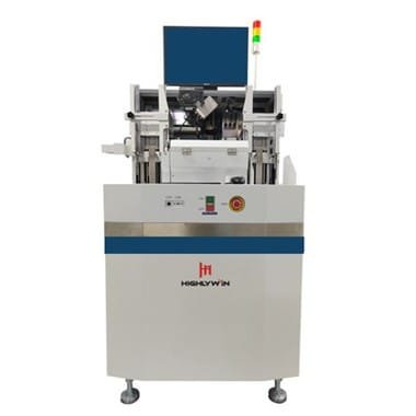
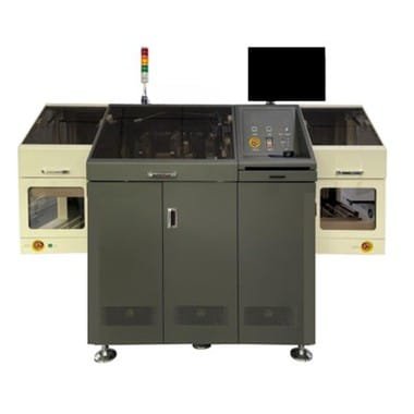
This HWS100-N high precision die bonder is a high accuracy system for LED products, suitable for SMD020, 1010,…
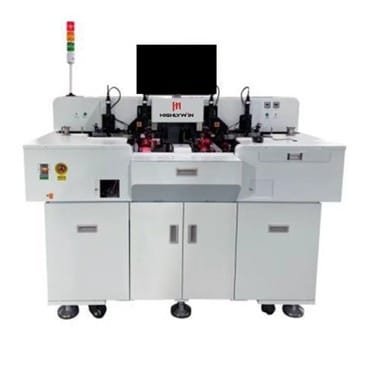
HW-BA60 aluminum wire bonding machines provide stable, fast, and efficient bonding solutions for high-power transistors, including the automotive electronics and home appliance industries.
Wire bonding machine is the method of making interconnections between an integrated circuit (IC) or other semiconductor device and its packaging during semiconductor device fabrication.
A die bonder is a system that places a semiconductor device onto the next level of interconnection, whether it be a substrate or a printed circuit board. It’s the process of fixing the wafer chip…
Wire Bonding and Die Bonding are two critical steps in the semiconductor packaging process, each playing an indispensable role in ensuring the electrical connections and physical stability of the chip. The Die Bonding Machine ensures the initial attachment and thermal management foundation for the chip, while the Wire Bonder is responsible for establishing critical electrical connections. Together, they ensure the performance, reliability, and production efficiency of semiconductor devices. Both steps are essential in the semiconductor packaging process, as they collectively determine the quality and functional integrity of the final packaged product.
Die Bonding is the first step in attaching the bare chip (Die) to the packaging substrate (such as a lead frame or PCB). This ensures that the chip has a stable position during the subsequent packaging process, providing a foundation for the structure of the entire integrated circuit.
By using appropriate adhesive materials (such as epoxy resin, metal alloys, etc.), Die Bonding aids in the thermal management of the chip, ensuring that heat can effectively transfer from the chip to the substrate, preventing overheating.
Die Bonding not only secures the chip but also provides initial mechanical support, protecting the chip from physical shocks, especially during the packaging process and in the final application.
Although Die Bonding itself does not directly create electrical connections, it provides the necessary platform for subsequent Wire Bonding or flip chip connections, serving as the starting point for electrical pathways.
Wire Bonding is a key step in establishing electrical connections between the chip and external circuits. It connects the pads on the chip to the packaging substrate or lead frame using gold, copper, or aluminum wires, ensuring the flow of signals and currents.
High-quality Wire Bonding is crucial for the long-term reliability of the package. It requires precise control to avoid short circuits, open circuits, or insufficient mechanical strength, ensuring stable operation of the product in actual applications.
Wire Bonding technology is applicable to various packaging types, from traditional packaging to more complex 3D packaging. Its flexibility supports different design requirements and cost-effective packaging solutions.
Compared to other connection technologies, such as bump connections for flip chips, Wire Bonding is generally more cost-effective in mass production, and the technology is mature and easy to implement.
SMT Machine One-stop Solution
Rm3A08 (4th Floor) Block D, Huashengtai Technology Park, No.36 Hangkong Road, Baoan District, Shenzhen City, China
© 2026 All Rights Reserved.