
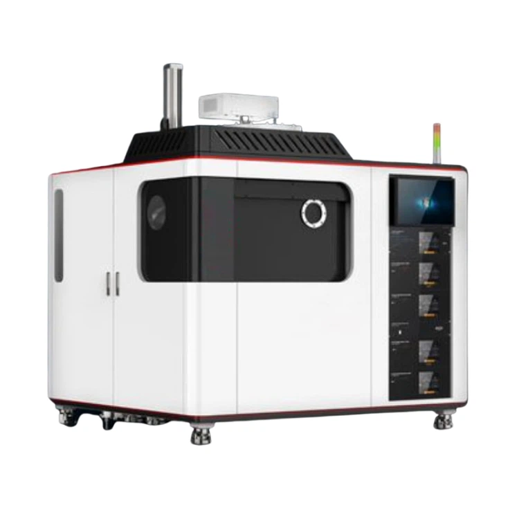
This is high-end equipment for the preparation of ultra-high precision optoelectronic devices. Focusing on high-quality optical coating, it has extremely low scattering value and defect density.
Ion beam etching (IBE) is a thin film technique that utilizes an ion source to carry out material removal processes on a substrate. IBE is a type of ion beam sputtering and, whether it’s used for…
Ion beam equipment plays an extremely important role in high-tech industries due to its advantages of high precision, low damage, versatility, and environmental friendliness, particularly in the fields of micro-nano manufacturing, materials science, and precision optics.
Ion beam equipment can provide extremely high positioning accuracy and energy control, making processing at the nanoscale possible. The focusing ability of the ion beam allows for precise etching or deposition of materials, which is crucial for manufacturing microelectronics, nanotechnology, and optical components.
Compared to traditional mechanical processing or thermal treatments, ion beam treatment causes less damage to materials. Since the ion beam strikes the surface with controllable energy, it reduces the heat-affected zone and avoids overheating the substrate, thereby maintaining the intrinsic properties of the material.
Ion beam etching can achieve selective removal of specific materials, which is particularly important for fine processing of multilayer structures, allowing for precise removal of upper materials without damaging the underlying layers.
During large-area processing, ion beam equipment can provide excellent uniformity, which is essential for manufacturing films that require strict thickness and surface quality.
Ion beam equipment is not only used for etching but also for assisted deposition, such as ion beam-assisted deposition (IBAD), making it highly flexible for preparing films with special properties, such as diamond-like carbon (DLC) coatings.
Ion beams can be used for cleaning and etching substrates, removing surface contaminants and providing a better surface condition for subsequent deposition or bonding.
Ion beam technology is suitable for various materials, including metals, ceramics, and semiconductors, which offers broad application potential across different industries.
By precisely controlling the parameters of the ion beam, high-purity films can be generated with reduced defects, which is crucial for the manufacturing of high-performance electronic and optical components.
SMT Machine One-stop Solution
Rm3A08 (4th Floor) Block D, Huashengtai Technology Park, No.36 Hangkong Road, Baoan District, Shenzhen City, China
© 2025 All Rights Reserved.