Introduction: A Manufacturing Revolution in the Microcosm
From smartphone processors and medical device control boards to automotive electronic sensors, the creation of this precision hardware relies on Surface Mount Technology (SMT). Compared to traditional Through-Hole Technology (THT), SMT has driven the electronics industry forward with three key innovations:
- Miniaturization: Component sizes have shrunk to 01005 (0.4×0.2mm), allowing for assembly densities several times higher than THT.
- High-Level Automation: Top-tier pick-and-place machines can achieve speeds of 250,000 CPH (Components Per Hour) with placement accuracy reaching the ±15μm level.
- High Reliability: Solder joints formed by reflow soldering offer superior mechanical strength and electrical performance, with consistency far exceeding manual soldering.
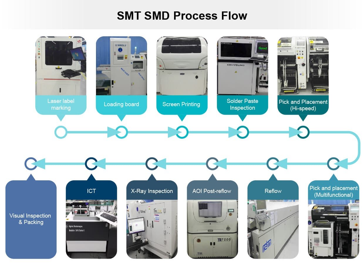
I. SMT Process Flowchart Overview
A complete SMT process operates like a precision assembly line where every stage is critical.
graph LR
    A[PCB Loading
(Loader)] --> B[Solder Paste Printing
(Printer)]
    B --> C[3D SPI
(Solder Paste Inspection)]
    C --> D[Component Placement
(Mounter)]
    D --> E[Reflow Soldering
(Reflow Oven)]
    E --> F[AOI
(Automated Optical Insp.)]
    F --> G{Has BGA/QFN
or other hidden joints?}
    G -- Yes --> H[X-Ray Inspection]
    H --> I[Unloading / Next Process]
    G -- No --> I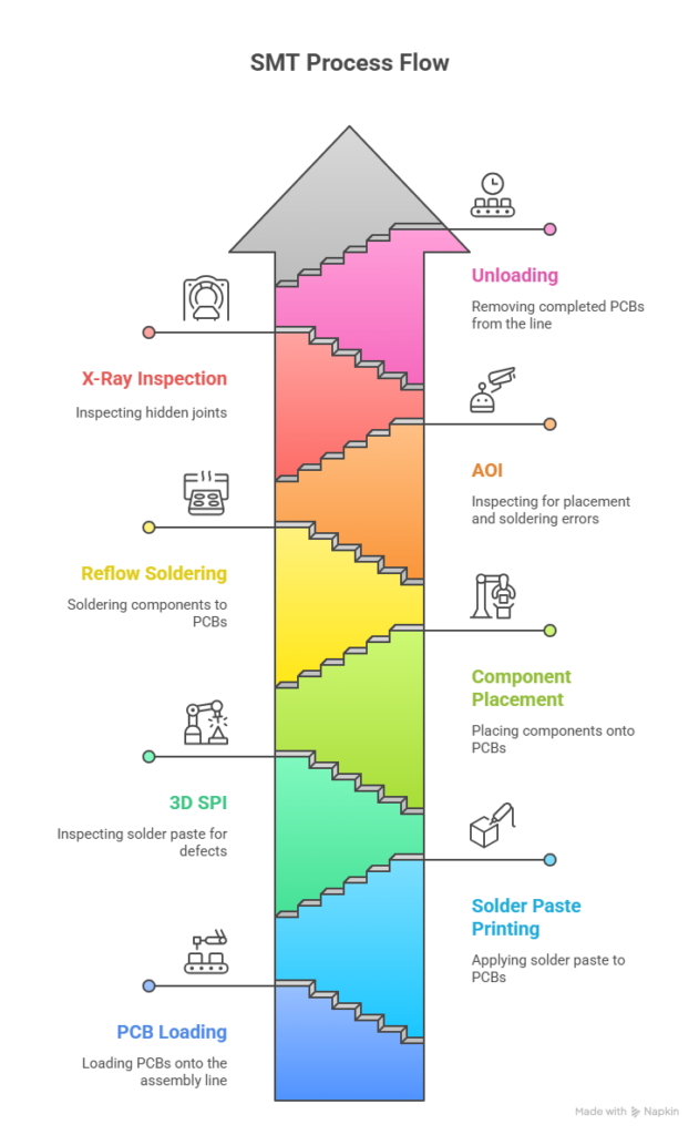
II. Core SMT Process Steps Explained
Step 1: PCB Loading and Pre-processing
- Key Equipment: Automatic PCB Loader
- Pre-processing Essentials:
- Baking for Dehumidification: Typically baking at 125°C for several hours to remove moisture from the PCB substrate and components, preventing “popcorning” (delamination) during high-temperature soldering.
- ESD Protection: The environment must have strict temperature and humidity controls (e.g., 45%-70% humidity), and all personnel must wear ESD wrist straps to protect sensitive components.
Step 2: Solder Paste Printing – Where Precision Dictates Success
This step precisely applies a defined amount of solder paste onto the PCB’s pads, preparing them for component soldering.
| Element | Example Technical Specs | Impact |
|---|---|---|
| Stencil | Laser-cut, aperture accuracy ±5μm, electro-polished | Ensures a high solder paste transfer efficiency (>90%) and a clean print definition. |
| Solder Paste | Type 4 powder size (20-38μm), viscosity 800-1000 kcps | Reduces risks of slumping and bridging after printing. |
| Squeegee | Polyurethane or metal, hardness 80-90 Shore A, angle 45°-60° | Guarantees uniform and consistent print thickness. |
Step 3: SPI – The First Line of Defense Against Soldering Defects
SPI (Solder Paste Inspection) uses 3D optical technology to inspect the volume, area, height, and shape of the solder paste on every pad, making it a critical process control point.
# Example logic for a solder paste inspection pass/fail check
def check_paste(paste_data):
    # Note: Thresholds are defined by specific product and process requirements.
    height_ok = 0.08 <= paste_data.height <= 0.15 # in mm volume_ok = paste_data.volume_percent >= 70
    area_ok = paste_data.area_coverage >= 80

    if height_ok and volume_ok and area_ok:
        return "PASS"
    else:
        # Trigger an alarm and prompt for stencil cleaning or parameter adjustment
        return "FAIL - Trigger Alarm"

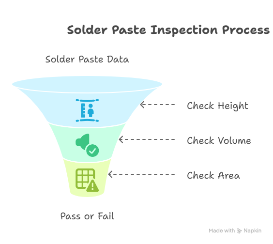
Industry statistics show that SPI can prevent over 70% of potential soldering defects caused by poor solder paste printing.
Step 4: Component Placement – A Game of Micron-Level Accuracy
- Key Equipment: Pick-and-Place Machine (or Mounter), available as high-speed chip shooters and high-precision flexible mounters.
- Core Technologies:
- Vision Alignment: Uses cameras to recognize fiducial marks on the PCB and component leads for high-precision placement (common accuracy is ±0.05mm).
- Nozzle Technology: Automatically changes nozzles based on component size and shape, picking them up with a vacuum system.
- Error-Proofing: Verifies component information by scanning barcodes on feeders to prevent wrong parts; uses on-the-fly cameras or laser sensors to check component orientation, preventing tombstoning or polarity reversal.
Step 5: Reflow Soldering – The Art of the Thermal Profile
The PCB, with components placed on it, travels through a tunnel-like oven with multiple heating zones. The solder paste melts and then cools to form reliable electrical and mechanical connections.
An Ideal Thermal Profile (Example for lead-free SAC305 solder):
graph TD
    A(Entry) --> B[Preheat Zone
Ramp to 150-180°C
60-90s]
    B --> C[Soak / Activation Zone
Hold at 180-220°C
60-120s]
    C --> D[Reflow Zone
Peak Temp 240-250°C
45-60s above liquidus]
    D --> E[Cooling Zone
Cooling Rate < 4°C/s]
    E --> F(Exit)

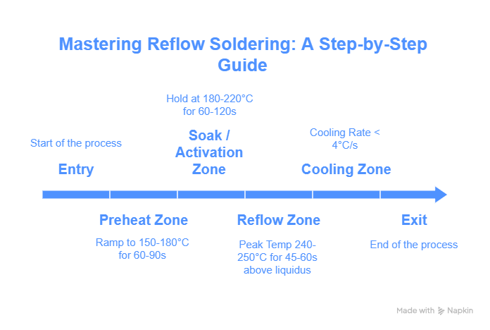
For high-density or heat-sensitive boards, Nitrogen (N₂) is often used to create an inert atmosphere. Keeping oxygen levels extremely low (e.g., <500 ppm) reduces oxidation and improves solder joint quality.
Step 6: AOI – The Intelligent Vision Inspector
AOI (Automated Optical Inspection) is performed after reflow to automatically inspect the PCBA for soldering defects.
- Defects Detected: Missing components, wrong parts, reversed polarity, component shift, tombstoning, bridging, solder balls, and insufficient solder.
- Technological Evolution: Modern AOI systems increasingly use AI algorithms based on deep learning. Trained on vast libraries of defect images, they significantly improve detection accuracy and reduce false calls.
Step 7: X-Ray Inspection (for Hidden Solder Joints)
For components like BGAs, QFNs, and LGAs with solder joints underneath the package, AOI is ineffective. X-ray inspection can penetrate the chip to clearly visualize the internal solder ball connections.
- Key Inspection Points: Solder shorts, open circuits (non-wets), and the size and percentage of voids (e.g., IPC standards may require voiding to be <25%).
III. Single-Sided vs. Double-Sided SMT: A Process Comparison
Depending on the product design, PCBAs can be single-sided or double-sided, with the latter involving a more complex process.
| Process Difference | Single-Sided Assembly | Double-Sided Assembly (Top first, then Bottom) |
|---|---|---|
| First Side (Top) Process | Full SMT Flow (Print → Place → Reflow) | Full SMT Flow (Print → Place → Reflow) |
| Board Flipping | N/A | Uses a dedicated inverter module in the line for a smooth transition. |
| Second Side (Bottom) Process | N/A | Another full cycle of Print → Place → Reflow. |
| Key Challenge | — | Controlling the second reflow profile to prevent components on the top side (now hanging upside down) from falling off, especially heavier ones. |
| Typical Application | Simpler boards like remote controls, power supplies. | High-density products like smartphone motherboards, laptops, and communication modules. |
IV. SMT Defect Analysis and Quality Fortification
Top 4 Defect Solutions
| Defect Type | Typical Root Cause | Corrective/Preventive Action |
|---|---|---|
| Tombstoning | Uneven thermal mass on the two pads of a component, causing solder to melt at different times. | Optimize PCB pad design for thermal symmetry (DFM); optimize the reflow preheat zone. |
| Solder Balls | Moisture in the solder paste or overly aggressive flux; preheat ramp rate is too fast. | Store and handle solder paste according to specifications; slow down the preheat ramp rate. |
| Cold Solder Joint | Insufficient peak temperature or time in the reflow zone; pad oxidation. | Optimize the reflow thermal profile; ensure good solderability of PCBs and components. |
| BGA Voiding | Flux volatiles fail to escape completely before the solder joint solidifies. | Use low-voiding solder paste; optimize stencil aperture design (e.g., window-panes); optimize the thermal profile. |
The Twin Pillars of Quality Systems
- DFM (Design for Manufacturability)
- Considering manufacturing process limitations during the product design phase, such as component spacing, pad design, and fiducial placement.
- IPC Standard Implementation
- Adhering to internationally recognized electronics assembly standards, such as IPC-A-610 (Acceptability of Electronic Assemblies) and J-STD-001 (Requirements for Soldered Electrical and Electronic Assemblies).
V. Emerging Trends in SMT
- Smart Factory & Industry 4.0: Connecting all equipment via an MES (Manufacturing Execution System) for real-time data monitoring, traceability, and intelligent decision-making to optimize OEE (Overall Equipment Effectiveness).
- Fine-Pitch and Heterogeneous Integration: Increasing demands for assembling sub-01005 components and high-density SiP (System-in-Package) modules.
- Green Manufacturing: Use of low-VOC or no-clean fluxes and energy-efficient equipment to reduce environmental impact.
Conclusion: The Path of Refinement Never Ends
When a high-density motherboard with thousands of components flows efficiently down an SMT line, it represents a perfect fusion of materials science, precision engineering, optics, and software. Mastering the core SMT process is the key to entering the world of modern electronics manufacturing. Only by continuously embracing technological innovation can one thrive on this path of constant improvement.
Appendix: Frequently Asked Questions (FAQ)
Q1: How do you choose a pick-and-place machine?
A: Key metrics include theoretical speed (CPH), real-world throughput (UPH), placement accuracy (μm), supported component range, and changeover time. The choice depends on a comprehensive evaluation of product type and production volume.
Q2: Is the adhesive (red glue) process obsolete?
A: In mixed-technology assembly (SMT + THT) requiring wave soldering, the adhesive process is still indispensable for securing SMT components. However, it is rarely used in purely double-sided reflow processes.
Q3: Is 100% SPI inspection necessary?
A: For high-reliability products (e.g., automotive, medical, aerospace) and high-density, fine-pitch PCBAs, 100% SPI is mandatory. The automotive industry often requires a process capability index (Cpk) of ≥ 1.67, which signifies an extremely low potential defect rate that can only be assured through 100% inspection.
Q4: How can reflow oven energy consumption be optimized?
A: Modern reflow ovens can be over 30% more energy-efficient than older models by using multi-stage heat recovery systems, improved insulation materials, and intelligent standby modes.
Take Action Now:
Get Your SMT Line DFM Checklist
Subscribe to our Electronics Manufacturing Weekly to unlock more process secrets!
(Note: Data in this article is cited from IPC standards, equipment technical white papers, and industry best practices. Some figures are typical examples; actual values depend on the specific process.)