Utiliza imágenes 3D para escanear la superficie, y la imagen escaneada se compara con las medidas especificadas para la placa. Este método es muy preciso para detectar defectos, lo cual es importante, ya que cualquier defecto puede provocar que la placa no funcione o falle prematuramente.
Esta inspección de pasta de soldadura 3D garantiza que las PCB se fabriquen correctamente al detectar la pasta de soldadura.


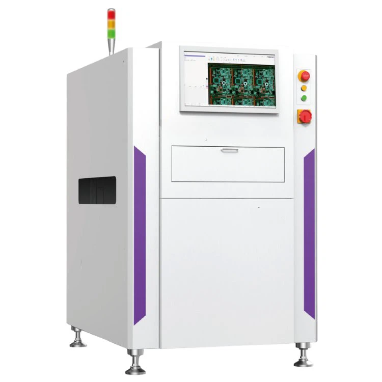
Modelo | Icono | Icono-D | |
Sistema de imágenes | Cámara | Cámara industrial de 5MP/12MP | |
Resolución | 5 MP: 15 μm, 20 μm; 12 MP: 5,5 μm, 10 μm, 12 μm, 15 μm | ||
Resolución de altura | 0,37 μm | ||
iluminación | LED en forma de anillo de 3 colores (RGB) | ||
Método de medición de la altura | proyectores | ||
Estructura del movimiento | Movimiento X/Y | Servomotor de CA | |
Plataforma | Granito | ||
Ajuste de la anchura | Automático | ||
Tipo de transporte | Cinturón | ||
Dirección de carga de la placa | L a R o R a L | ||
Carril fijo | Carril único: 1.er carril fijo; Carril doble: 1.er y 3.er o 1.er y 4.º carril fijo | ||
Configuración del hardware | Sistema operativo | Win10 | |
Comunicación | Ethernet, SMEMA | ||
Potencia | Monofásico 220V, 50/60Hz, 5A | ||
Necesidades de aire | 0,4-0,6Mpa | ||
Altura de la cinta | 900±20mm | ||
Tamaño total | 1000 mm x 1360 x 1620 mm | ||
Peso del equipo | 950 kilos | 1000 kilos | |
Manejo de la placa | Tamaño PCB | 50*50-510*610 mm | Carril único: 50 x 50-510 x 320 mm |
Altura máxima de la almohadilla | 600 μm | ||
Espaciado mínimo de almohadillas | 100 μm (dentro de una altura de 150 μm) | ||
Tamaño máximo de la pasta de soldadura | 20*20 mm | ||
Tamaño mínimo de la pasta de soldadura | 0,1 mm | ||
Borde de sujeción | 3 mm | ||
GR&R | ≤10% | ||
Función de inspección | Defectos | Carámbano, soldadura insuficiente, exceso de soldadura, altura promedio, desplazamiento, puente de soldadura, forma extraña, cobre expuesto, dedo dorado, etc. | |
Velocidad de inspección | 400-450 ms/campo de visión | ||
Solución integral para máquinas SMT
Rm3A08 (4th Floor) Block D, Huashengtai Technology Park, No.36 Hangkong Road, Baoan District, Shenzhen City, China
2026 Todos los derechos reservados.