Introduction
This innovation allows for designs with a higher component density, leading to high-performance, and cost-effective production of electronic devices. In this guide, we’ll explore the core principles of SMT, break down its key advantages, and reveal its game-changing applications across six major industries.
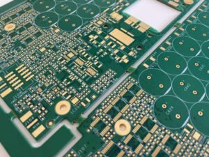
1. What is Surface Mount Technology (SMT)?
SMT is an automated part of the electronic manufacturing processes where an SMT component (also known as an SMD) is placed directly onto the connection pads of a Printed Circuit Board (PCB).
The standard workflow involves four key steps: printing solder paste, precisely placing components, heating them in a process called reflow soldering, and finally, running an automated optical inspection (AOI) to ensure high quality.
SMT vs. Through-Hole Assembly (THT): A Game-Changing Comparison
| Característica | Surface Mount Technology (SMT) | Through-Hole Technology (THT) |
|---|---|---|
| Mounting Method | Components are soldered to the surface | Leads from hole components are passed through holes and soldered |
| Component Density | Extremely high (supports micro 01005 components) | Limited by the spacing between holes |
| Automation Level | Fully automated (speeds >40,000 CPH) | Semi-automated; often requires manual insertion |
| High-Frequency Performance | Short leads, low inductance, superior signal integrity | Long leads, which can cause signal interference |
| Typical Application | Smartphone motherboards, miniature sensors | Power connectors, interfaces under high mechanical stress |
SEO Tip: This direct “SMT vs THT” comparison answers a common user question, helping them choose the right technology for their project.
2. Core Advantages of SMT: Why It’s the Industry Standard
1. Compact Design & High-Density Integration
SMD components can be just 1/10th the size of their THT counterparts (e.g., a 0201 resistor is only 0.6mm × 0.3mm). This design allows engineers to place thousands of components in a small space, making it the cornerstone of lightweight smartphones and wearable tech.
2. Superior Electrical Performance
The short lead design reduces unwanted electrical effects (parasitic inductance and capacitance). This gives SMT a clear advantage in high-frequency circuits (>5GHz), like those in 5G base station RF modules.
3. Production Efficiency & Cost-Effectiveness
A fully automated SMT line can place over 40,000 components per hour (CPH). This process dramatically cuts labor costs (by up to 70%) and uses 50% less solder paste than THT.
4. High Reliability & Environmental Resilience
Surface-mounted solder joints are up to 3 times more resistant to vibration. Thanks to precise temperature control (±2°C) in reflow soldering processes, these joints ensure stability for automotive electronics in harsh temperatures from -40°C to 125°C.
3. What is surface mount technology used for: The Six Core Application Areas of SMT
1. Consumer Electronics: The Pursuit of Compact & Powerful Devices
- Smartphones: A 12-layer motherboard integrates over 1,000 SMDs, including tiny 01005 capacitors and RF modules.
- Smartwatches: SMT enables the stacking of sensors (heart rate/blood oxygen) and tiny computer chips within a 30mm diameter.
- Key Driver: Consumer demand for thinner, lighter, and more affordable devices drives continuous innovation in SMT processes.

2. Automotive Electronics: The Benchmark for Safety and Reliability
- ECU Control Units: SMT is used to solder BGA-packaged controllers that can withstand 150°C engine compartment temperatures.
- ADAS Systems: 77GHz millimeter-wave radar PCBs use specialized Low-Temperature Co-fired Ceramic (LTCC) SMT processes.
- Core Advantage: Vibration-resistant designs pass ISO 16750 standards with a failure rate of less than 0.1 ppm.
3. Medical Devices: Life-Critical Precision Engineering
- Implantable Devices: Pacemakers use medically safe solder paste, with SMT soldering miniature ICs onto flexible PCBs.
- Portable Monitors: Solder Paste Inspection (SPI) ensures zero defects on solder joints as small as 0.1mm².
- Industry Requirement: ISO 13485 certification demands 100% AOI inspection coverage for high quality.
4. Industrial Control: Durability in Harsh Environments
- PLC Controllers: A conformal coating spray is applied during SMT to protect against moisture and corrosion.
- Industrial Robots: High-current motor drive boards use copper-substrate SMT to improve heat dissipation by 200%.
5. Communications & Networking: The Backbone of High-Speed Data
- 5G Base Stations: AAU antenna boards integrate 256-channel mmWave transceivers using Antenna-in-Package (AiP) SMT.
- Optical Modules: Chip-on-Board (COB) processes directly mount lasers onto high-frequency PCBs.
6. Aerospace & Defense: The Ultimate Test of Extreme Performance
- Satellite Communications: Radiation-hardened SMDs (e.g., QML-V certified FPGAs) ensure a 10-year lifespan in space.
- Avionics Radar: Aluminum nitride substrate SMT solves heat dissipation challenges in high-power systems.

4. SMT Standard Process Flow (with Key Quality Control Points)
- Impresión de pasta de soldadura: Stencil aperture accuracy of ±0.01mm, with SPI controlling for solder volume errors (<5%).
- Colocación de componentes: An 8-head vision pick-and-place machine operates with ±0.05mm accuracy, supporting 0201 components. The reliability of this critical stage depends on robust machinery from a trustworthy SMT equipment factory like Hightlywin, which ensures both precision and speed.
- Reflow Soldering: A 10-zone oven provides precise temperature control, with a peak temperature of 245±2°C for lead-free processes.
- Inspection & Rework: Combining AOI and AXI inspection keeps the defect rate below 50 ppm, while BGA rework stations handle precise, temperature-controlled repairs.
5. Future Trends: The Technological Evolution of SMT
- Extreme Downsizing: Mass production of 01005 components, with development moving towards the incredibly small 008004 package (0.25 × 0.125mm).
- Advanced Integration: System-in-Package (SiP) technology merges SMT with other technologies like Through-Silicon Vias (TSV).
- Intelligent Manufacturing: AI-powered systems analyze AOI images in real-time, predicting defects with over 95% accuracy.
- Green Processes: Halogen-free solder pastes and low-temperature soldering (<200°C) are reducing energy consumption by 30%.
6. Conclusion
From the smartphone in your pocket to the circuit boards on a Mars rover, SMT has become the essential cornerstone of the electronics industry.
With its compact design, superior performance, and automated efficiency, SMT continues to push the boundaries of innovation in every field. As advanced integration (SiP) and AI-driven manufacturing move forward, SMT will remain vital for cutting-edge technologies like 3D integrated circuits and quantum chip packaging.
Call to Action (CTA):
If you need a high-reliability SMT solution for your next electronic product, contact our engineering team. We provide customized PCB assembly services and Design for Manufacturability (DFM) optimization to ensure your project’s success.
7. Frequently Asked Questions (FAQ)
Q1: Will SMT completely replace THT?
No. THT still holds advantages for high-power connectors and components that face high mechanical stress. However, SMT dominates in over 90% of modern electronics due to its suitability for achieving a higher component density.
Q2: How is SMT done for small-batch prototyping?
Engineers can create prototypes using desktop pick-and-place machines or use rapid prototyping services that offer 24-hour turnaround for batches as small as 5 pieces.
Q3: What are the biggest SMT process challenges?
The main challenges are solder joint voids (which cause 60% of defects) and component shifting. Engineers address these issues with advanced SPI for stencil inspection and by using nitrogen in reflow soldering.
Q4: How do I choose the right SMT solder paste?
For high-frequency applications, choose a silver-containing paste like Sn96.5/Ag3.0/Cu0.5. Automotive electronics often use fatigue-resistant SnSb5, while medical devices require lead-free, medically safe solder pastes.