Points de repère dans la conception des circuits imprimés
Les points de marquage, également appelés points optiques ou points de référence, sont essentiels pour identifier les positions sur les circuits imprimés lors de l'assemblage des composants. Leur sélection a un impact direct sur l'efficacité des machines de placement automatique, ce qui nécessite une conception rigoureuse des points de marquage et de leur emplacement sur la carte.
Conception des points de repère
1. Position de la disposition
Points de marque du tableau unique
Lors de la conception de circuits imprimés, les points de repère doivent être ajoutés du côté où le composant doit être placé. Pour un placement double face, les points de repère doivent être ajoutés des deux côtés, idéalement aux quatre coins, de manière asymétrique pour éviter tout décalage. Si l'espace est limité, trois points de repère peuvent suffire ; toutefois, au moins deux points de repère doivent être ajoutés en diagonale si nécessaire.
Points de repère du panneau
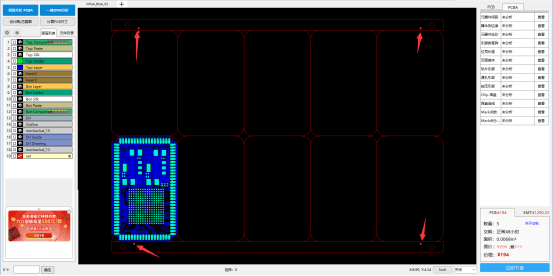
Les panneaux nécessitent également des points de marquage, placés à chacun des quatre coins du bord de traitement, afin d'éviter tout placement symétrique et d'éviter toute erreur. Si le panneau n'a pas de bord de traitement, des points de marquage doivent être ajoutés directement sur la planche. Si aucun point de marquage n'est ajouté à une pièce, au moins trois points de marquage doivent être placés dans les espaces vides des panneaux connectés.
Points de repère des composants
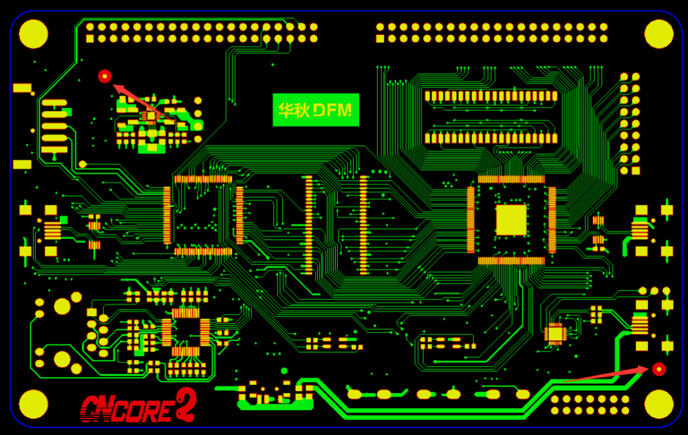
Pour améliorer la précision de placement de certains composants, tels que les QFP et les BGA, des points de marquage dédiés doivent être ajoutés, positionnés à deux coins diagonalement opposés l'un à l'autre sur le composant.
2. Spécifications de conception
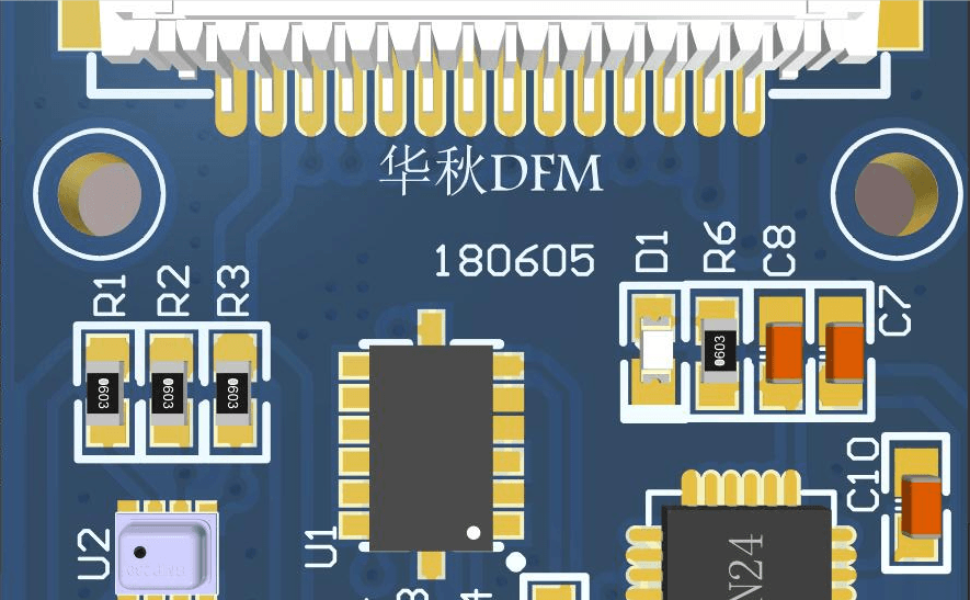
Forme et taille
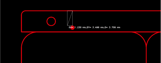
Les points de marquage peuvent être circulaires ou carrés, généralement de 1,0 mm, avec une ouverture du masque de soudure de 2,0 mm. Pour éviter tout reflet gênant sur la détection des points de marquage, l'ouverture doit dépasser la ligne PAD de plus de 0,5 mm. Dans les espaces restreints, une ouverture de 1,5 mm est autorisée, mais la ligne PAD doit dépasser 1,0 mm.

Distance du bord
La distance de sécurité entre les points de marquage et le bord de la planche doit être supérieure à 3,5 mm afin d'éviter toute obstruction par le convoyeur pendant le traitement. S'ils sont situés sur le bord de la planche, ils peuvent être ajustés vers l'intérieur, garantissant ainsi que les points de marquage internes restent à au moins 3,5 mm du bord.
Espaces ouverts
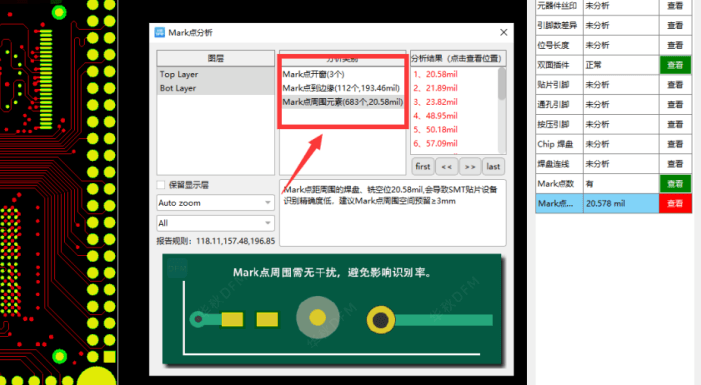
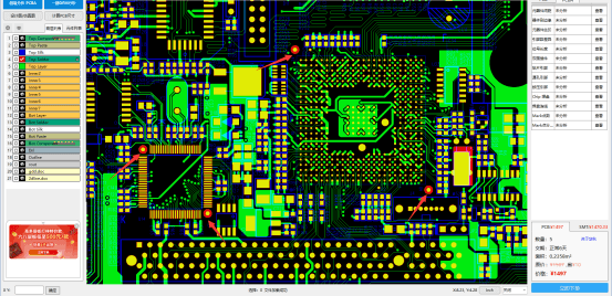
Évitez de placer des pistes ou des composants à proximité des points de marquage, car cela affecte la reconnaissance. Un espace libre de plus de 3 mm doit être prévu autour de chaque point de marquage pour garantir une précision optimale de l'équipement de placement CMS.
Application des points de repère dans SMT
Principe d'utilisation du Mark Point
Lors du placement, un désalignement peut survenir. Le positionnement par point de repère permet de remédier efficacement à ce problème en servant de référence. Les machines de placement équipées de la fonctionnalité de point de repère permettent de mieux déterminer le positionnement précis des composants, garantissant ainsi une grande précision de positionnement.
Méthodes de placement sans points de marquage
En l'absence de points de repère pour le placement automatique, il est possible de sélectionner une pastille de soudure spécifique comme point de repère. Utiliser un pochoir ou créer un montage avec un point de repère peut constituer une autre méthode ; cependant, la précision sera probablement compromise sans les points de repère traditionnels.
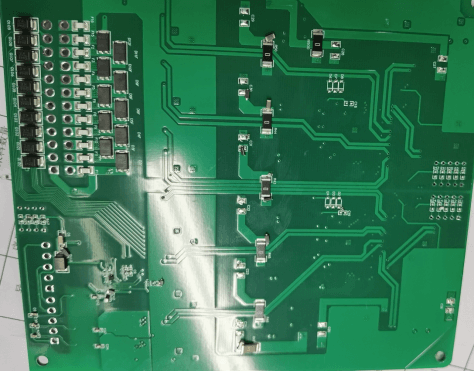
Cas de production sans points de marquage
Description du problème
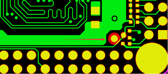
L'absence de points de marquage a conduit à une mauvaise identification des points, entraînant un placement incorrect des composants.
Impact du problème
Un placement incorrect a entraîné la perte de plusieurs composants, retardant le développement du produit et gaspillant les coûts de R&D et de fabrication.
Extension du problème
Un placement incorrect des composants en raison de l'absence de points de marquage peut entraver la fonctionnalité du produit, nécessitant une nouvelle production et un réapprovisionnement des composants pour l'assemblage.
Solutions d'inspection Mark Point
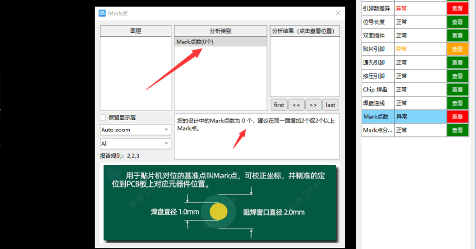
L'utilisation du logiciel DFM de Huachiu pour inspecter les points de marquage permet d'éviter les pertes de développement produit dues à des points de marquage manquants ou mal conçus. La vérification des fichiers de conception avant la conception peut réduire les coûts de R&D et les cycles de production.
Partie 1
Le logiciel DFM de Huachiu détecte si des points de repère manquent dans les fichiers de conception. En cas d'absence, le logiciel indique la nécessité de points de repère pour servir de références de positionnement aux machines de placement, permettant ainsi des coordonnées corrigées et un positionnement précis sur les circuits imprimés.
Partie 2
Le logiciel DFM de Huachiu permet également d'identifier les anomalies dans les conceptions de points de marquage. Les contrôles incluent la taille de l'ouverture du point de marquage, la distance de sécurité par rapport aux bords et l'influence des objets environnants sur la reconnaissance du point de marquage. Ce logiciel répond à diverses exigences d'inspection de conception.