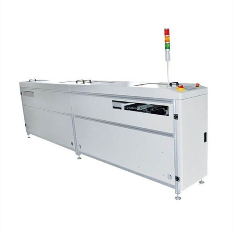
The inspection conveyor is used when frequent visual inspection of PCB’s is required in the PCB assembly line. It also used for connecting between SMT production machines.
This series device is using at the terminal of the SMT PCB production line for automatic unloading of PCBs.

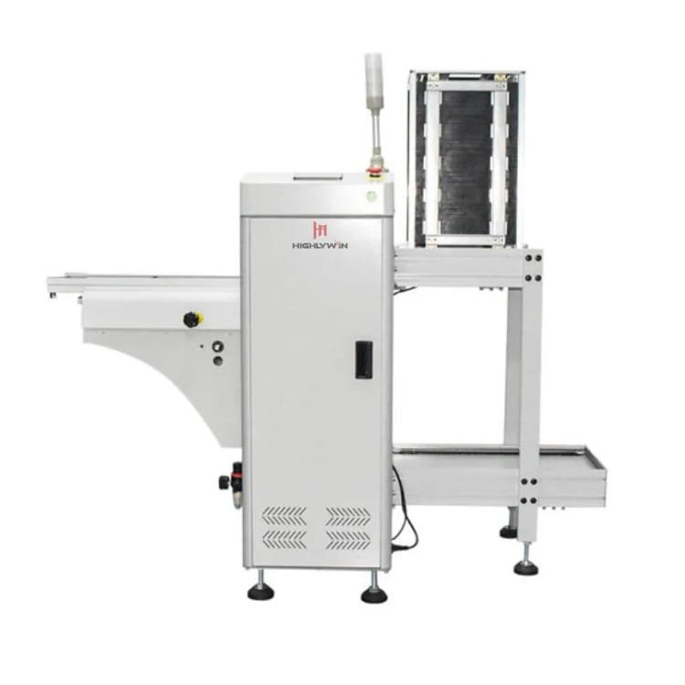
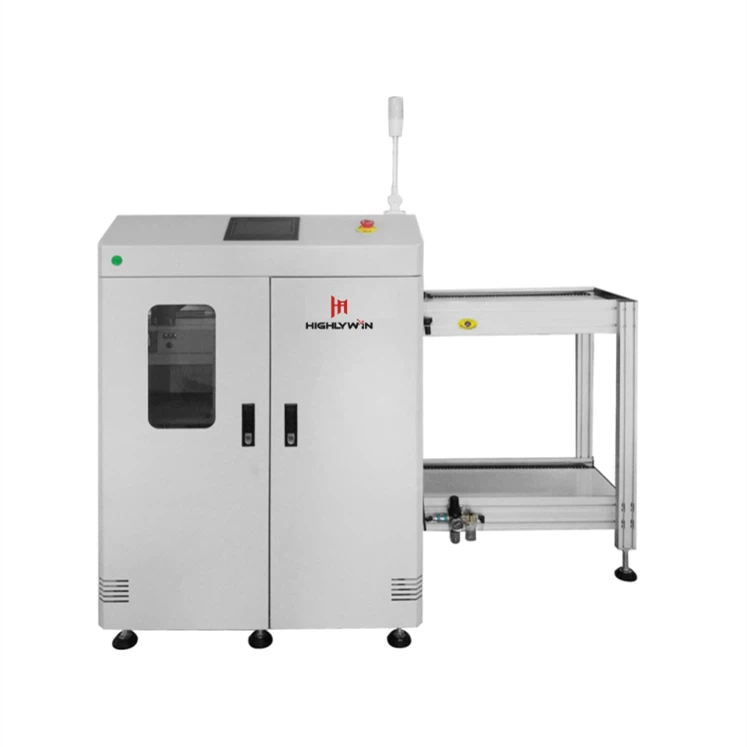
This series loader is designed for automatic loading of PCBs in SMT production lines. The unit loads PCB automatically after receiving the board signal from the host.

This SMT buffer is used for NG/OK board caching and re-judgment of PCB boards on SMT production line, usually used after the SPI/AOI machine in the automatic SMT line.
This equipment is used for shunting and merging of multi-line on SMT production lines, and dislocation translation transfer between single-line equipment.
This unit is designed for loading/unloading the bare boards onto/off the SMT line in a high speed.

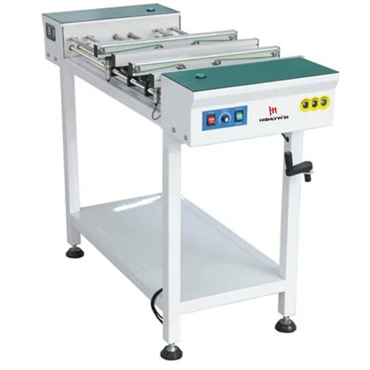
This unit removes the PCB top surface dirt particles, glass fiber, and eliminates the static electricity before solder paste, adhesive application, and after laser marking.
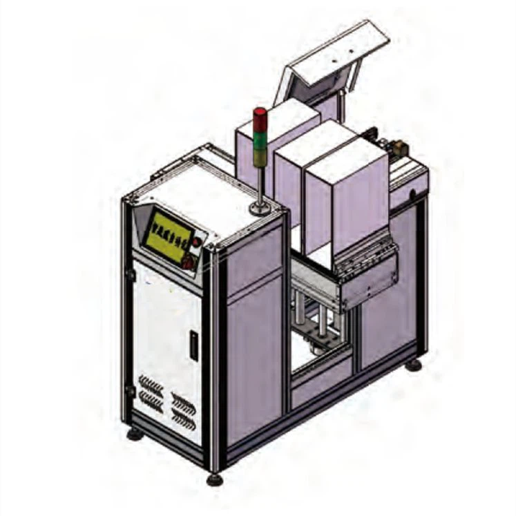
This BGA loading and unloading machine is mainly used for semiconductor packaging and testing, washing the front end of the line body, and transferring the BGA board to the following equipment…

This high-quality wave soldering conveyor loader/unloader is used to handle a wide range sizes and shapes of PCB/PCB with jig, ensures smooth and efficient transfer of boards through the wave…
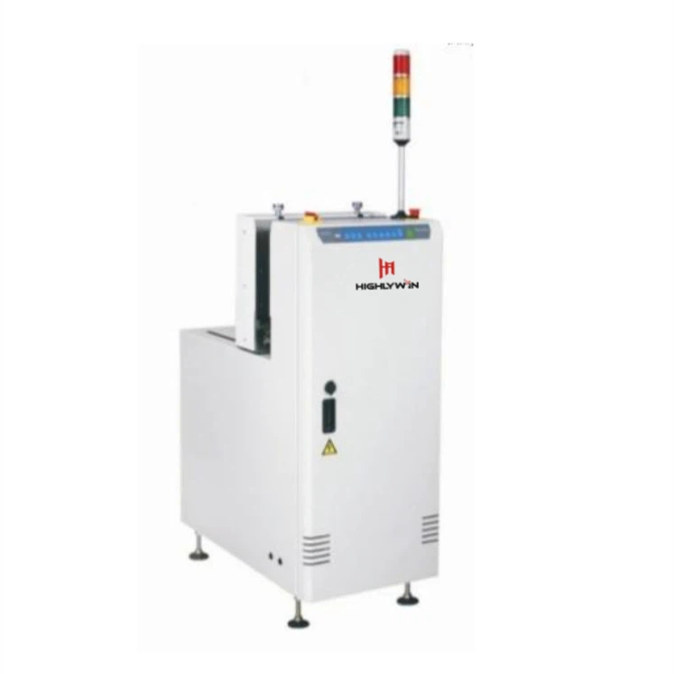
This NG reject conveyor is available to automatically separate the OK/NG board signal from the upstream SPI/AOI test machine and can lift the NG PCB for visual inspection without stopping or…

This unit is used to transfer PCBs around corners for continued process flow. Available in clockwise or counterclockwise rotation, and by-pass mode are selectable.

This Telescopic Gate Conveyor is used for creating a passage in the PCB intelligent assembly line to give the operator access to the rear of the production equipment. The integrated conveyor…

This NG reject conveyor is available to automatically separate the OK/NG board signal from the upstream SPI/AOI test machine and can lift the NG PCB for visual inspection without stopping or…
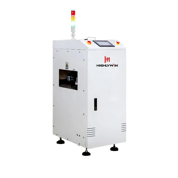
This unit removes the PCB top surface dirt particles, glass fiber, and eliminates the static electricity before solder paste, adhesive application, and after laser marking.
The necessity of PCB Handling Equipment in SMT and PCB manufacturing is evident in its ability to improve production efficiency, ensure product quality, adapt to different PCB sizes and shapes, support high-density and high-performance PCBs, reduce costs, enhance reliability, and support rapid prototyping. The application of these devices and technologies not only promotes the development of the electronics industry but also brings higher competitiveness and economic benefits to enterprises.
Automation: Key equipment in SMT production lines, such as screen printers, pick-and-place machines, and reflow ovens, significantly enhances production efficiency through automation. For example, screen printers can accurately apply solder paste on PCB pads in a short time, while pick-and-place machines can mount hundreds of components within minutes.
Reducing Human Error: Automated equipment minimizes operational errors, improving the stability and consistency of production. Especially in large-scale manufacturing, manual operations can lead to fatigue and oversight, resulting in decreased product quality.
Precise Control: PCB Handling Equipment can accurately control the position and orientation of PCBs, ensuring that each step is executed correctly. For instance, pick-and-place machines utilize high-precision vision systems and robotic arms to ensure that every component is placed in the correct position.
Quality Inspection: AOI (Automated Optical Inspection) equipment can conduct detailed inspections of PCBs after reflow soldering, identifying and marking defects such as poor solder joints or missing components, thus ensuring the quality of the final products.
Flexibility: Equipment in SMT production lines can accommodate various sizes and shapes of PCBs. For irregularly shaped PCBs, techniques such as panelization or adding process edges of at least 8 mm in the long direction of the PCB can meet equipment requirements.
Size Limitations: Although SMT equipment has certain size limitations for PCBs, optimal layout plans can maximize the use of existing machinery. Currently, the smallest PCB shape commonly processed in SMT production lines is 90 mm x 50 mm (length x width), while the maximum dimension should not exceed 350 mm x 250 mm. If designs require exceeding these dimensions, layout solutions can be negotiated with engineering staff.
Miniaturization of Vias: As SMT technology advances, the size of vias on PCBs has gradually reduced from 0.8 mm to 0.3 mm or even smaller. This not only increases PCB density but also enables the support of more high-density packaged components such as BGAs (Ball Grid Arrays) and QFPs (Quad Flat Packages).
Buried/Blind Via Structures and via-in-pad: These technologies significantly enhance the density and performance of PCBs. Buried and blind vias allow for more complex electrical connections in multilayer boards, while via-in-pad further improves panel flatness and coplanarity, reducing warpage and enhancing soldering quality and reliability.
Reducing Material Waste: Precise control by automated equipment can reduce waste of solder paste and adhesives, thus lowering material costs.
Simplifying Production Processes: The use of automated equipment streamlines production processes, minimizing steps requiring manual intervention and lowering production costs. For instance, using acrylic boards instead of solder paste stencils can significantly reduce production time and costs.
Soldering Reliability: SMT technology, through processes like reflow soldering, ensures the reliability and stability of solder joints. This is especially critical for high-density packaged components like BGAs, where the design and precise placement of pads are vital for soldering reliability.
Environmental Adaptability: SMT technology allows PCBs to better adapt to various environmental conditions, such as high temperatures and humidity. For example, surface treatments like chemical nickel/gold, chemical tin, and chemical silver can enhance the solderability and corrosion resistance of pads, extending the lifespan of PCBs.
Quick Sampling: In laboratory environments, adding equipment like laser engravers, 3D printers, PCB etching machines, and heat transfer printers can facilitate rapid prototyping of PCBs. This not only accelerates product development cycles but also allows designers to promptly verify and adjust design plans.
Customized Designs: These devices can also support the customization of PCB shapes and product appearances according to specific requirements, catering to various application scenarios.
SMT Machine One-stop Solution
Rm3A08 (4th Floor) Block D, Huashengtai Technology Park, No.36 Hangkong Road, Baoan District, Shenzhen City, China
© 2026 All Rights Reserved.