Vision Systems in Pick-and-Place Machines
Modern pick-and-place vision systems serve as the “eyes and brain” of electronic manufacturing equipment, combining advanced imaging hardware with intelligent software to achieve micron-level precision in component placement. This guide covers system architecture, core functions, technological evolution, and detailed model comparisons.
I. System Architecture
1. Hardware Components
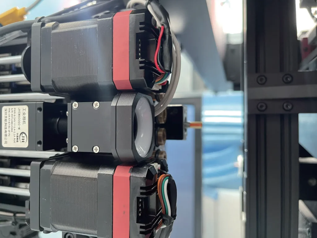
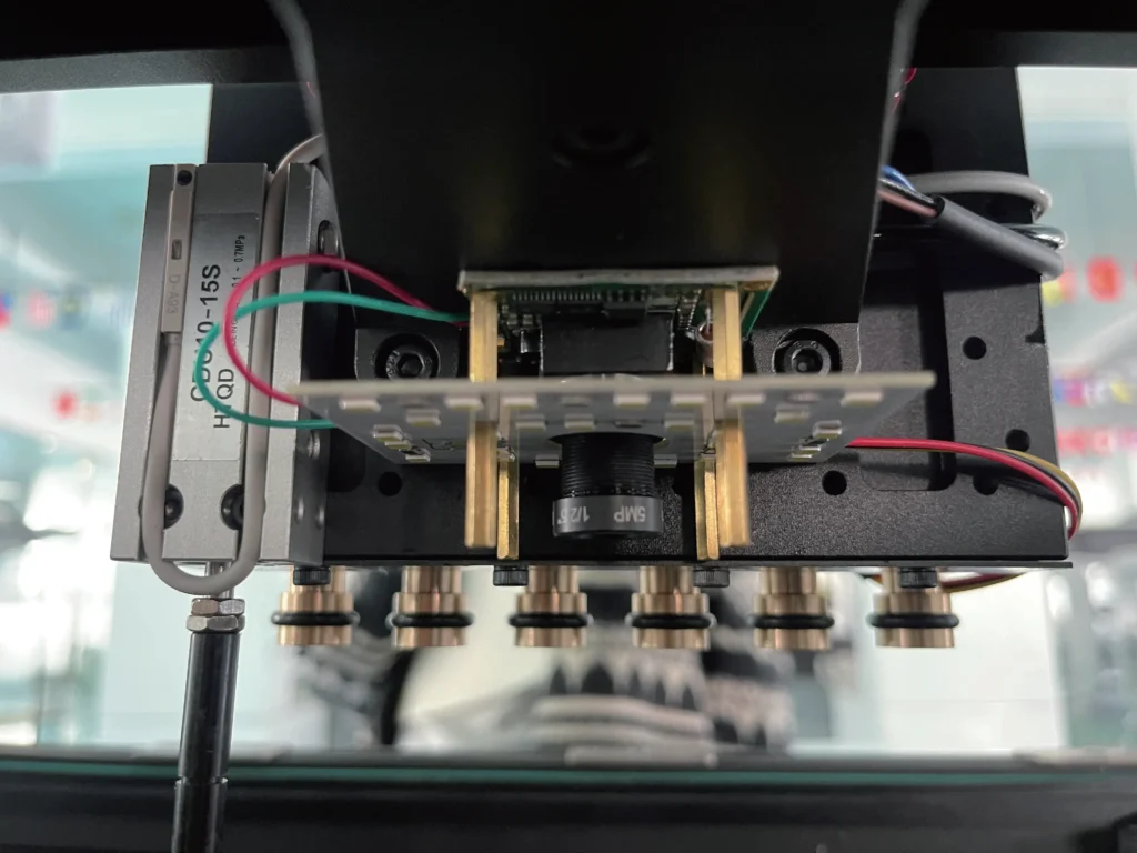
- Industrial Cameras:
- Line scan cameras (for high-speed recognition)
- Area array cameras (for precise positioning, e.g. 5MP MARK camera in HW-F5)
- Lighting Systems:
- Ring lights, coaxial lighting (dual-source in HW-S6 for material adaptability)
- Scattering light sources for component contrast enhancement
- Auxiliary Sensors:
- Laser rangefinders (PCB warpage detection)
- Vacuum self-check sensors with visual confirmation
- Torque sensors in collaborative robot applications

2. Software Algorithms
- Image processing (edge detection, template matching)
- Deep learning models (defect prediction, path optimization)
- Coordinate transformation systems (image-to-mechanical mapping)
- WYSIWYG PCB simulation interfaces
II. Core Capabilities
1. Component Recognition & Positioning
- High-speed flying cameras capture 0402 (0.4×0.2″) to 0201 micro components
- Handles challenging conditions: blurred silkscreen, tilted components (HW-S6 enhanced algorithms)
- 360° component rotation with 0.1° precision (HW-A8)
2. Calibration & Compensation
- Nozzle center calibration (±0.05mm accuracy)
- Real-time PCB warpage compensation (laser measurement + auto-adjustment)
- Thermal expansion correction (environmental drift compensation)
- Spline-guided Z-axis movement for consistent focus (HW-S6)
3. Quality Control
- Pre-placement checks: polarity verification, lead deformation
- Post-placement 3D inspection: solder pad contact validation
- Component library management systems
III. Technology Evolution
1. Precision Advancements
- From 0.1mm (2000s) to 0.02mm today (HW-F5 0201 support)
- Laboratory systems achieving micron-level precision
2. Intelligent Features
- Rule-based algorithms → Machine learning → Deep learning
- MES integration for production data tracking
- AI-powered path optimization (HW-F5/S5)
3. Multi-Sensor Fusion
- Force sensors for placement pressure monitoring
- Spectral analysis for material verification
- Collaborative robotics with vision-guided obstacle avoidance
Emerging Technologies: Event-based cameras (100,000+ CPH), quantum dot sensors for low-light environments, and hybrid vision-force control systems.
IV. Model Comparison: HW Series Vision Systems
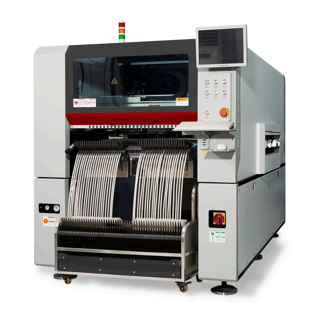
Pick-and-Place Machine
| Feature | HW-A8/A6L | HW-F5/S5 | HW-S6 |
|---|---|---|---|
| Camera System | 8 linear cameras (A8) 6×400K pixel (A6L) | Hybrid: Flying + Linear + Fixed 500W MARK camera | 5MP flying + 6MP MARK Dual light sources |
| Min. Component | 0402 (11mm) | 0201 (0.6×0.3mm) | 0201 with enhanced recognition |
| Speed | 15,000 CPH (A6L) | 84,000 CPH (S5 dual-arm) | 45,000 CPH |
| Special Features | Basic component library | AI path optimization Thermal compensation | Spline Z-axis Through-hole feeders |
| Applications | Entry-level SMT | High-mix microelectronics | Demanding precision tasks |
V. Application Scenarios
1. LED Manufacturing
- 3528/5050 large LEDs on flexible substrates (HW-A8L)
- Requires scattering light sources for contrast
2. Microelectronics Packaging
- 0201 resistors/capacitors, QFN chips
- Demands 6MP+ cameras for pin verification
3. Power Devices
- 40×40mm MOSFET/IGBT modules
- Special nozzles and lighting configurations required
Selection Criteria: Balance speed (CPH), precision (μm), and component compatibility. High-volume production benefits from HW-S5’s dual-arm configuration, while R&D environments may prefer HW-S6’s enhanced recognition capabilities. (Data references: IEEE Industrial Electronics Society publications 1990-2023 & HW technical documentation)