Маркировочные точки при проектировании печатных плат
Точки отметки, также известные как оптические точки или опорные точки, имеют решающее значение для определения позиций на печатных платах во время сборки компонентов. Их выбор напрямую влияет на эффективность автоматических машин для размещения, что требует тщательного проектирования точек отметки и их расположения на плате.
Дизайн точек отметки
1. Расположение макета
Очки за одиночную доску
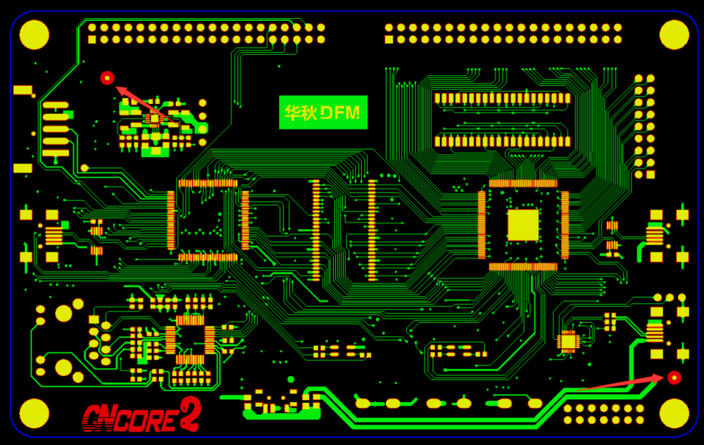
При проектировании печатных плат точки Mark должны быть добавлены на сторону, требующую размещения компонентов. Для двухстороннего размещения точки Mark должны быть добавлены на обе стороны, в идеале на все четыре угла в асимметричном расположении, чтобы предотвратить несоответствие. Если пространство ограничено, может быть достаточно трех точек Mark; однако, по крайней мере, две следует добавить по диагонали, если необходимо.
Точки отметки панели
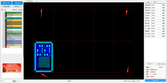
Панели также требуют точек Mark, с точками в каждом из четырех углов кромки обработки, избегая симметричного размещения для защиты от дурака. Если панель не имеет кромки обработки, точки Mark следует добавлять в саму доску. Когда точки Mark не добавляются к одной детали, по крайней мере три должны быть размещены в пустых областях соединенных панелей.
Компонент Марк Очки
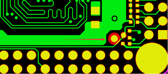
Для повышения точности размещения определенных компонентов, таких как QFP и BGA, следует добавить специальные точки маркировки, расположенные в двух углах компонента по диагонали друг напротив друга.
2. Технические характеристики конструкции
Форма и размер
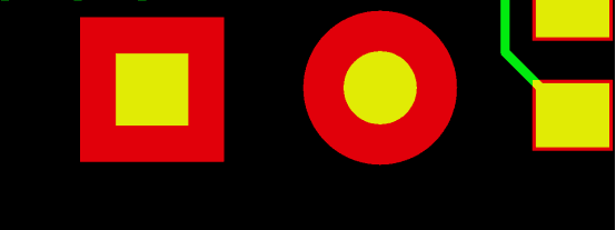
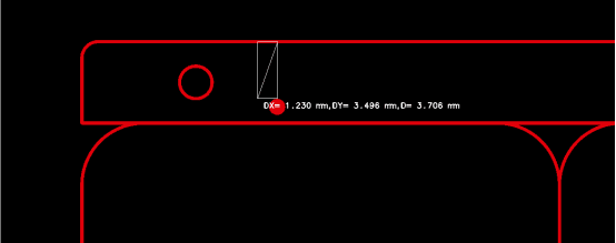
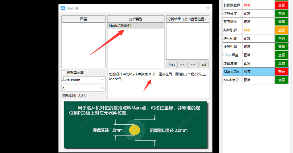
Точки отметки могут быть круглыми или квадратными, обычно размером 1,0 мм, с отверстием паяльной маски 2,0 мм. Чтобы избежать бликов, влияющих на обнаружение точки отметки, отверстие должно превышать линию PAD более чем на 0,5 мм. В ограниченном пространстве допускается отверстие 1,5 мм, но линия PAD должна превышать 1,0 мм.
Расстояние до края
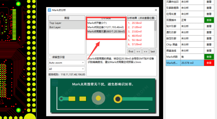
Безопасное расстояние точек Mark от края доски должно превышать 3,5 мм, чтобы предотвратить помехи со стороны конвейера во время обработки. Если они расположены на краю обработки, их можно отрегулировать внутрь, гарантируя, что внутренние точки Mark останутся на расстоянии не менее 3,5 мм от края.
Открытые пространства
Избегайте размещения дорожек или компонентов вблизи точек отметки, поскольку это влияет на распознавание. Вокруг каждой точки отметки следует установить зону зазора более 3 мм, чтобы обеспечить оптимальную точность для оборудования для размещения SMT.
Применение баллов Mark Points в SMT
Принцип использования точки отметки
В процессе размещения может возникнуть несоосность. Позиционирование точки отметки эффективно решает эту проблему, выступая в качестве ориентира для размещения. Машины для размещения, оснащенные функциональностью точки отметки, могут лучше определять точное размещение компонентов, обеспечивая высокую точность размещения.
Методы размещения без отметок точек
При отсутствии точек Mark для автоматического размещения можно выбрать определенную контактную площадку в качестве точки Mark. Альтернативным методом может служить наклеивание трафарета или создание приспособления с точкой Mark; однако точность, скорее всего, будет снижена без традиционных точек Mark.
Производственные случаи без баллов
Описание проблемы
Отсутствие точек отметки приводило к неправильной идентификации точек, что приводило к неправильному размещению компонентов.
Влияние проблемы
Неправильное размещение привело к потере множества компонентов, задержке разработки продукта и напрасной трате средств на НИОКР и производство.
Проблема Расширения
Неправильное размещение компонентов из-за отсутствия точек маркировки может ухудшить функциональность изделия, что потребует повторного производства и повторного поиска компонентов для сборки.
Решения для инспекции Mark Point
Использование программного обеспечения DFM компании Huachiu для проверки точек отметки может предотвратить потери при разработке продукта из-за отсутствия или неправильного проектирования точек отметки. Проверка файлов проекта перед проектированием может сократить расходы на НИОКР и производственные циклы.
Часть 1
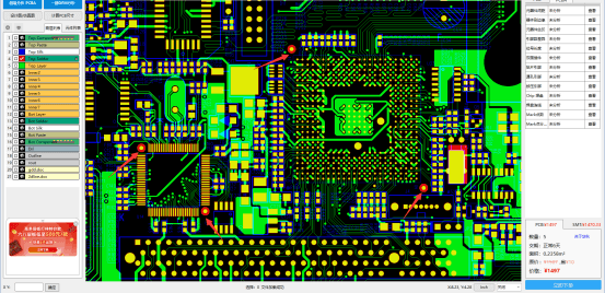
Программное обеспечение DFM компании Huachiu определяет, отсутствуют ли в файлах дизайна точки отметки. Если они отсутствуют, программное обеспечение укажет на необходимость использования точек отметки в качестве опорных точек позиционирования для машин размещения, что позволяет корректировать координаты и точно размещать детали на печатных платах.
Часть 2
Программное обеспечение DFM компании Huachiu также может определять отклонения в проектах Mark point. Проверки включают размер отверстия Mark point, безопасное расстояние до краев и влияние окружающих объектов на распознавание Mark point. Это программное обеспечение может выполнять различные требования к проверке дизайна.
Производитель машин для поверхностного монтажа печатных плат