Ion Beam Etching (IBE)
Ion Beam Etching is a highly precise surface modification technique used in microfabrication and nanotechnology. This technology employs a focused beam of high-energy ions, typically generated from a plasma source, to selectively remove material from a substrate’s surface. Here are the key aspects of IBE technology:
Key Aspects
- Precision and Uniformity: IBE allows for the creation of extremely precise patterns and structures with high uniformity across the substrate. This is due to the controllability of the ion beam, which can be directed and focused accurately.
- Material Selectivity: The process is suitable for a wide range of materials, including metals, oxides, semiconductors, and even organics. It can etch chemically sensitive materials without causing unwanted damage to the surrounding areas.
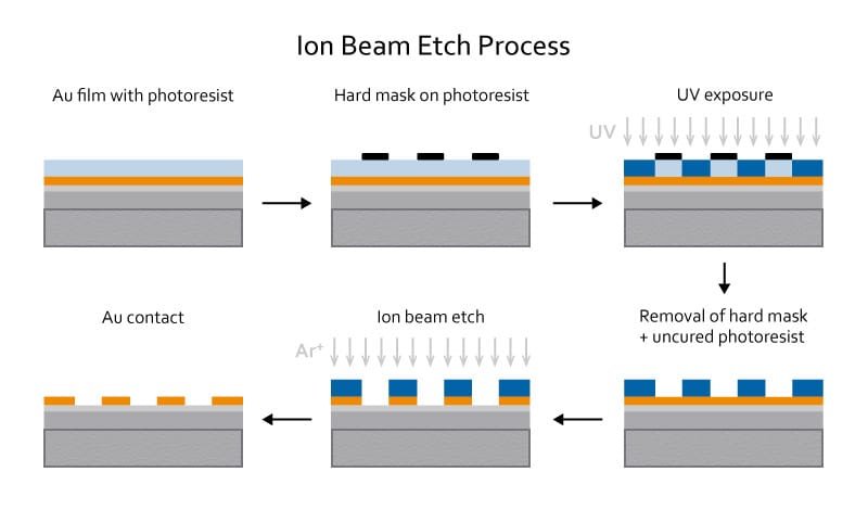
- Etching Mechanism: The etching rate depends on factors such as the ion flux, sputtering yield (the efficiency of material removal per ion impact), and the density of the material being etched. The ions, usually argon or other noble gases ionized under RF fields, physically knock atoms off the surface. In practice, users often need to optimize these parameters according to material and design requirements to achieve the best etching rate and selectivity, which includes adjusting the ion beam energy, flux density, and etching time.
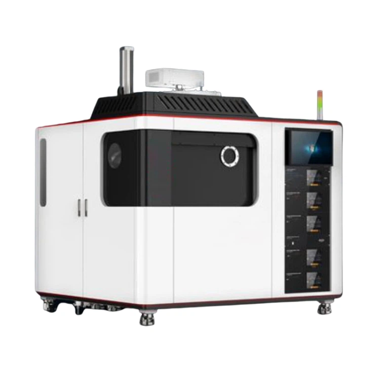
- Ion Beam Source Components: The system comprises a discharge chamber where a gas is ionized, grids that control the ion beam’s extraction and direction, and a neutralizer to balance the charge. This setup ensures a controlled flow of ions towards the substrate.
- Masking: Like other etching techniques, IBE often uses a mask to protect certain areas of the substrate, allowing for pattern transfer. The mask’s pattern determines the structure that will be etched. In some complex micro/nano-structure manufacturing processes, multiple steps of ion beam etching may be required to achieve more intricate geometries or features, which is commonly seen in integrated circuit manufacturing and MEMS (micro-electro-mechanical systems) applications.
- Приложения: IBE is crucial in the semiconductor industry for creating microelectronic components, such as integrated circuits, where fine features and tight tolerances are essential. It’s also used in the development of thin-film applications and for modifying surface properties in various research and industrial contexts.
- Advantages Over Other Etching Techniques: IBE offers better anisotropy, meaning it etches vertically rather than laterally, which is critical for maintaining feature integrity in high aspect ratio structures. It also reduces the risk of redeposition of etched material, a common issue in other etching methods. However, despite its high selectivity, practitioners must monitor for potential side reactions or increased surface roughness that can occur, as these may impact the overall process quality.
- Экологический контроль: The environmental control, such as the vacuum level and gas composition during the IBE process, is crucial for ensuring etching consistency and quality. A good vacuum environment helps minimize undesired gas molecule interference, thus enhancing etching precision.
- Conclusion and Future Directions: As material science and equipment technology continue to advance, the application scope of IBE may further expand. The emergence of novel ion sources and control systems may propel its use in biomedical materials, optoelectronic devices, and nanostructures.
In summary, Ion Beam Etching is a sophisticated technique that leverages the power of ion beams to create intricate patterns and structures at the micro and nanoscale, making it a vital tool in advanced manufacturing and research.
lon Beam Etching Equipment for PCB and SMT