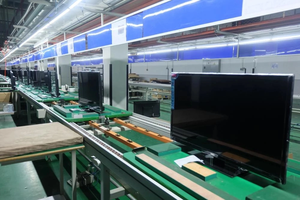
Smart TV SMT Assembly Line Solutions
Design Goals: Adapted for smart TV motherboards from 55 to 85 inches (maximum size 500×300mm), supporting precise assembly needs such as Mini LED backlight driver circuits, HDMI 2.1 high-speed interfaces, achieving ±15μm mounting accuracy, and compatible with ultrathin 0.3mm PCBs and 01005 micron components.
1. Core Equipment Configuration and Selection
| Equipment Category | Key Technical Parameters | Function Adaptation |
|---|---|---|
| Solder Paste Mixer | 10L large capacity mixing tank, dual spiral vacuum defoamer (viscosity control ±3Pa·s), supports low-temperature solder (Sn42Bi58) | Continuous feeding for large motherboards |
| SMT Loader | Four-track independent feeding, maximum load 600×400mm, speed ≥1000 boards/hour (includes automatic board edge cleaning) | Mixed line production for multiple-size TV motherboards |
| Solder Paste Printer | Screen adaptive tension control (±0.1N), printing accuracy ±12μm, supports 0.2mm spacing Mini LED pads | High-density backlight driver circuit printing |
| SPI Machine | Multi-wavelength 3D detection (405nm+650nm), solder paste volume detection resolution 0.01mm³, AI auto-compensation for printing parameters | Mini LED micro pad defect interception |
| Pick and Place machine | Fuji NXT III dual-track model (refurbished), accuracy ±20μm, supports 120×90mm large suction nozzles | SOC chip and interface component mounting |
| Micro Component Feeding System | Vibratory feeders + 0201 precision feeders, waste rate <0.08% (includes RFID material tracking) | Power management module mounting |
| Reflow Machine | 14-temperature zones, adjustable chain speed 0.5-2.0m/min, supports RSS curve (ΔT≤1.5℃/zone) | Control of thermal deformation for large motherboards |
| AOI Machine | Multi-spectral imaging (12 combinations of light sources), deep learning algorithms to detect cold solder/jump, false positive rate <0.25% | Full inspection of PCB and data tracking |
| X-Ray Inspection Machine | Micro-focus 1μm resolution, supports BGA solder ball 3D modeling, automatic determination of void ratio (threshold <5%) | Verification of SOC chip soldering quality |
| Selective Wave Soldering | Dynamic nitrogen-protected wave, adaptive soldering angle (±3°), supports 0.4mm pitch connectors | HDMI/USB interface soldering |
| Precision Dispensing Machine | Nano-level injection valve (dispense volume 0.003ml), supports simultaneous operation of bottom-filling glue and thermal grease | Assembly of chip thermal management modules |
| Laser Marker | UV laser (355nm), adjustable marking depth 0.02-0.2mm, supports binding of MAC address and production batch | Full lifecycle tracking of products |
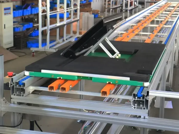
| Docking Station | Heavy-duty six-axis adjustable platform, maximum load 80kg, compatible with MES system for real-time interaction | Precise docking for large motherboards |
| SMT Unloader | Intelligent sorting system (OK/NG/Repair), automatic generation of repair work orders for NG products | Quality closed-loop management |
2.Smart TV SMT Production Line Layout and Capacity Optimization
1. Dedicated Layout for Large Motherboards
[Production Line Topology]
Loader → Printer → SPI → Docking Station → PnP (NXT III×2) → Reflow → AOI → X-Ray
↓
Wave Soldering ← Dispensing Machine ← Laser Marking ← Unloader
Key Design:
- Anti-Warping Solution: The printing section is equipped with a board preheating platform (45±2℃) and supporting jigs added before the reflow soldering section.
- Dual-Track Asynchronous Production: Track A produces main control boards (8-layer HDI) while Track B produces power boards (4-layer FR4).
- Static Protection System: Key positions equipped with ion blowers (balance ±5V) and anti-static curtains (surface resistance 10^6-10^9Ω).
2. Capacity Model and Efficiency Indicators
| Indicator | Parameter | Optimization Measures |
|---|---|---|
| Theoretical Mounting Speed | 68,000 CPH (NXT III×2) | Dual-track asynchronous production increases equipment utilization by 18% |
| Actual Capacity (OEE 84%) | Single shift (8h) output of 28,000 motherboards | Intelligent feeding system reduces downtime |
| Changeover Time | ≤25 minutes (quick change screen + recipe cloud synchronization) | Magnetic suction screens + recipe database fetching |
| Overall First Pass Yield | ≥99.3% (fourfold detection interception) | Optimized via AOI and X-Ray data linkage |
3. Special Process Support for Smart TVs
1. Mini LED Backlight Process
- Precision Mounting: Dedicated suction nozzles (contact area >90%) paired with pressure feedback systems (0.3-3N dynamic adjustment)
- Solder Control: Reflow soldering profile set with stepped temperature rise (2℃/s→1℃/s) to reduce thermal stress on LED chips.
- Optical Detection: SPI adds an infrared thermal imaging module for real-time monitoring of solder joint temperature uniformity.
2. High Thermal Dissipation Requirements Solution
Process Chain: Thermal grease dot coating → Heat sink pressing → Aging test (85℃/85%RH, 48h)
Equipment Support: Dispensing machine integrated with two-component mixing module (thermal conductivity ≥5W/m·K)
4. Cost Control and Value-Added Services
| Strategy | Implementation Plan | Benefits |
|---|---|---|
| Refurbished Equipment | NXT III vision system upgraded to 20μm, reflow soldering thermal compensation module replaced | Reduce costs by 35%, accuracy reaches 85% of new machines |
| Domestic Replacement Solutions | HW-G6 pick-and-place machine + Matrix VisionX AOI combination, supporting IPC-CFX standards | Overall investment reduced by 30% |
| Intelligent Maintenance System | Predictive maintenance module (vibration/temperature sensors) + cloud fault library | Reduce MTTR to 1.8 hours |
| Process Package Support | Provide “Smart TV Soldering Curve Library” (including parameters for mainstream models like Samsung/LG/Hisense) | Shorten trial production cycle by 5 days |
5.Smart TV SMT Machine Supplier Cooperation Framework
| Terms | Content |
|---|---|
| Acceptance Standards | Continuous 72-hour fault-free operation, key indicators: Mounting Cpk ≥1.67 / Solder void rate <4% |
| Spare Parts Guarantee | Spare parts center in East/South China, A-class parts (laser heads/servo motors) delivered within 6 hours |
| Technical Training | Provide “Large PCB SMT Process Manual” + 7 days on-site debugging (including ESD special measures) |
Attachments
- Smart TV motherboard thermal deformation simulation report (ANSYS analysis data)
- Mini LED mounting precision verification report (CPK ≥1.73)
- Refurbished equipment MTBF certification (≥12,000 hours)
This proposal optimizes large-sized PCB processes and specialized technologies for Mini LEDs, meeting the high precision and thermal dissipation needs of smart TVs. The triple cost control strategy reduces initial investment by 25%. It is recommended to prioritize the validation of the Mini LED soldering process while concurrently applying for UL/CE certification and HDMI 2.1 compatibility testing.