It uses 3D imaging to scan the surface area, and the scanned image is compared to the specified measurements for the specific board. This method is very accurate for detecting defects, which is important because any defect can lead to the board not working or failing early.
This 3D solder paste inspection ensures that PCBs are made correctly by detecting the solder paste.


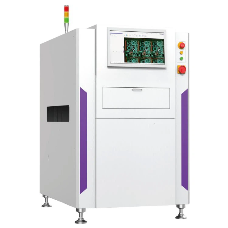
Model | Icon | Icon-D | |
Image System | Camera | 5MP/12MP industrial camara | |
Resolution | 5MP: 15μm, 20μm; 12MP: 5.5μm, 10μm, 12μm, 15μm | ||
Height Resolution | 0.37μm | ||
lighting | 3 color ring shape LED (RGB) | ||
Height measurement method | projectors | ||
Movement structure | X/Y movement | AC Servo | |
Platform | Granite | ||
Width adjustment | Automatic | ||
Transport type | Belt | ||
Board loading direction | L to R or R to L | ||
Fixed rail | Single lane: 1st fixed rail; Dual-lane: 1st & 3rd or 1st & 4th fixed rail | ||
Hardware configuration | Operating system | Win10 | |
Communication | Ethernet, SMEMA | ||
Power | Single phase 220V, 50/60Hz, 5A | ||
Air requirement | 0.4-0.6Mpa | ||
Conveyor height | 900±20mm | ||
Overall size | 1000mm*1360*1620mm | ||
Equipment weight | 950kg | 1000kg | |
Board handling | PCB Size | 50*50-510*610mm | Single lane:50*50-510*320mm |
Max pad height | 600μm | ||
Min pad spacing | 100μm (within height of 150μm) | ||
Max solder paster size | 20*20mm | ||
Min solder paster size | 0.1mm | ||
Clamping edge | 3mm | ||
GR&R | ≤10% | ||
Inspection function | Defects | Icicle, insufficient solder, excess solder, average height, offset, solder bridge, odd shape, exposed copper, golden finger, etc. | |
Inspection speed | 400-450ms/FOV | ||
SMT Machine One-stop Solution
Rm3A08 (4th Floor) Block D, Huashengtai Technology Park, No.36 Hangkong Road, Baoan District, Shenzhen City, China
© 2026 All Rights Reserved.